Interference and diffraction: simulations using spherical waves
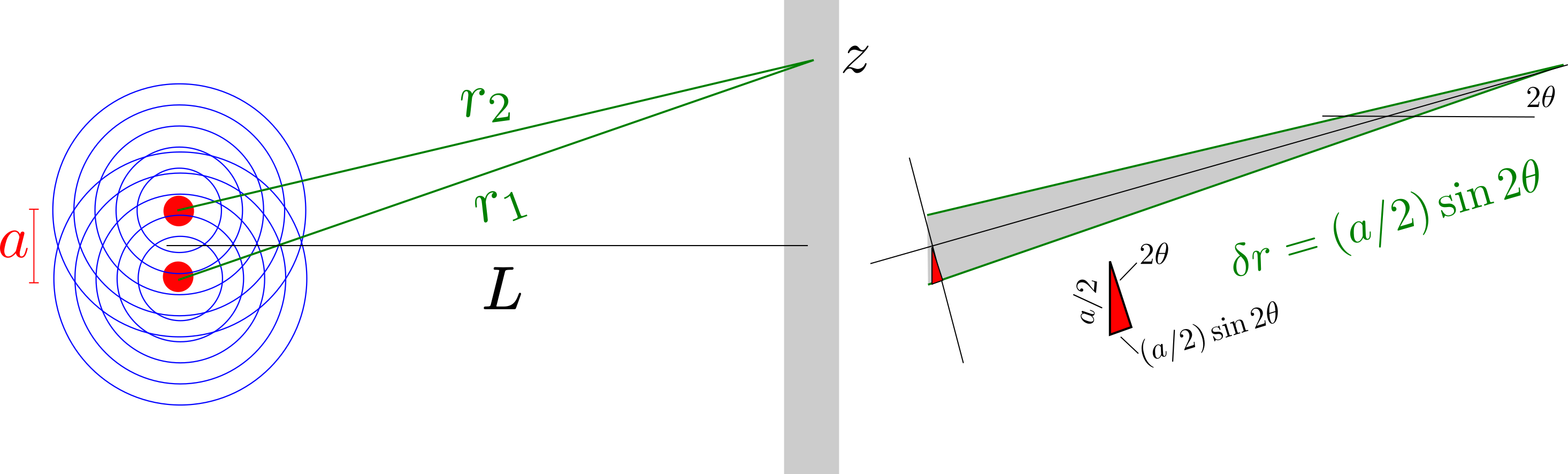
Assume that there are \( N \) scatterers, uniformly spaced by \( a \), with total length \( (N-1) a \): a finite lattice. The lattice could be a diffraction grating made by optical lithography (probed by visible light, like a laser pointer) or a crystal lattice (probed by x-rays or electron waves, as in a transmission electron microscope.) In this simple simulation, we will consider scatterers arranged in only one dimension, which could correspond to atomic planes in three dimensions.
The simulation assumes that each scatterer is a point source for a spherical light wave, radiating outwards from the point, with wavevector \( \mathbf{k}=k\hat{\mathbf{r}}\) in the radial direction, defined from the center of the scatterer.
You will see that a diffraction pattern emerges for the right choice of parameters. The diffraction pattern is equivalent to the spatial Fourier transform of the lattice. Since atomic spacings (periodicities) are characteristic of elements, this allows us to determine a material's composition.
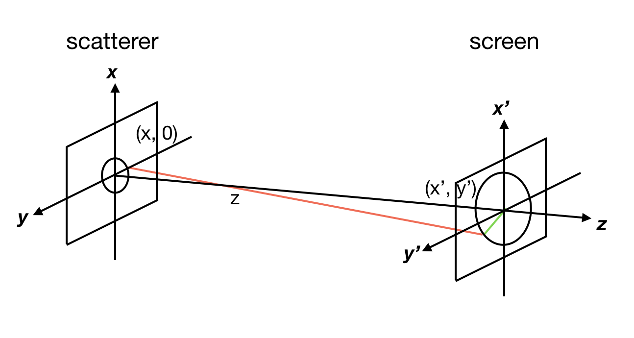
Consider the wave front on the screen is $$ \begin{equation} \begin{split} \tilde{E}(x', y') &= \frac{ a }{ r } \exp(i k r) \\ &= \frac{ a }{ \sqrt{(x - x')^2 + y'^2 + z^2} } \thinspace \exp \Big( i k \sqrt{(x - x')^2 + y'^2 + z^2} \Big) \\ &= \frac{ a }{ \sqrt{(x - x')^2 + y'^2 + z^2} } \bigg( \cos \Big(k\sqrt{(x - x')^2 + y'^2 + z^2} \Big) + i \sin \Big(k \sqrt{(x - x')^2 + y'^2 + z^2} \Big) \bigg), \end{split} \end{equation} $$ where \( (x', y') \) is the position of one image point, \( (x,0) \) is the position of one scatterer. See the figure below. Sum the E-field generated by each scatterer: we find \( \tilde{E}_\text{total} (x', y') \). The intensity \( I (x', y') = \tilde{E}_\text{total} \tilde{E}_\text{total}^\ast \).
Simulator
Questions
- Set \(N=2\) and \(N=4\). Compare (qualitatively) the intensity pattern for the light very close to the particles (short \(L\)) with that far away (long \(L\)).
- Set camera length \(L=\) to a few m. You will see regions on the screen where the light is intense, but mostly regions where it is not intense at all. How can you predict the location of the intense regions? (using what law?)
- Set \(a=\text{10} \mu \text{m}\), \(L=\text{5} \text{m}\), wavelength \(\lambda=\text{700} n\text{m}\). What is the smallest spacing on the screen between peaks in the intensity?
- If the interparticle spacing is doubled, what happens to the peak spacing (and why?) Justify your answer.
- If blue light is used instead -- assume 400 nm, what happens to the spacing (and why?) Justify your answer.
- Increase the number of particles \(N\). What happens to the height of the peaks? (Can you come up with a rule to predict the peak height as a function of \(N\)?)
- Increase the number of particles \(N\). What happens to the width of the peaks? (Can you come up with a rule to predict the peak width as a function of \(N\)?